
±10um Placement
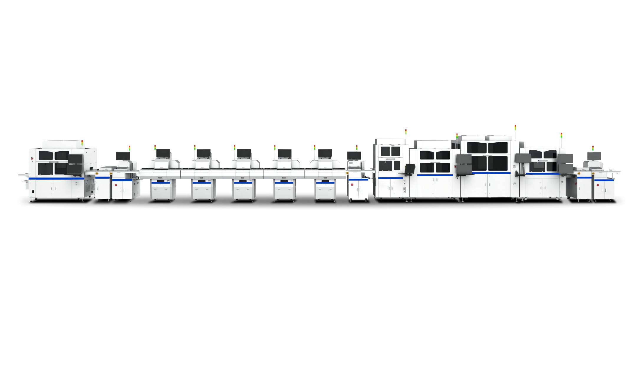
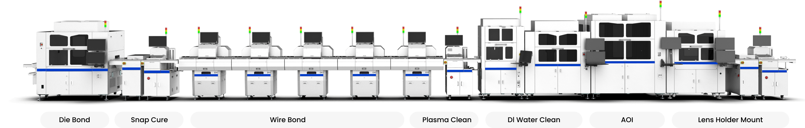
Die Attach & Flip Chip
0 Defect for Automotive Application

High Cleanness Control Class 10
Dispensing Process Expertise
7+ Years Stable & Reliable HVM

+30% High Throughput
Continuously Mass Production
Fully Automated Load/Unload

Flexible Configurations
SECS/GEM Traceability
Turnkey Solution
| Item | Specifications |
| End Market | Consumer/Automotive |
| Application | CCM/Automotive/IOT-COB, 3D-ToF, Fingerprint Sensor, IR Camera Module, VCM etc. |
| Material Handling | 4~12" Wafer, JEDEC Tray, Waffle Pack, etc. |
| Process | Dispensing, Jetting, Stamping, DAF |
| Die Placement | ±10um @3σ |
| UPH | Material Dependent |
| Footprint & Weight | Configuration Dependent |
Placement
Thin Die
Stacking
100


±5um Placement
Frictionless Precise Force Control
Vibration Suppression
25um Die Thickness
32-Hi Stacking
Key OSAT/IDM Running HVM

Leading UPH & OEE
Customized Functions
DAF & Epoxy Writing

Crack Free
Deep Learning Driven Vision
Support Industry 4.0
| Item | Specifications |
| Wafer | 6" ~ 12" |
| Die Size | 0.8 ~ 25mm |
| Die Thickness | ≥ 25um |
| Strip Length | 130 ~ 300mm |
| Strip Width | 55~100mm (Optional <55mm ) |
| Bond Force | 0.5 ~ 50N (70N optional) |
| Die Placement | ±5um @3σ |
| Item | Specifications |
| Process | DAF & Epoxy Dispensing |
| Cycle Time | Material Dependent |
| Heater Block | Max 250 ℃ (±5 ℃) |
| Die Stacking | YES |
| Packages | BGA/QFP/QFN |
| Footprint | 2292 x 1551 x 1900mm |
| Weight | 2450kg |
Placement
UPH
Flexibility
Footprint


±3um Placement
Qualified in Worldwide #1 Account
Advanced Packaging Solution

Optional High Force 50kg
Pre-Sintering SiC Die Attach
Modulization Design

Die Attach, Flip Chip, Stack Die, Multi Chip Mount
On The Fly Post Bond Inspection
Dual Mode (Speed/Precision)

Excellent Cleanliness Control
SECS/GEM Traceability
Support Industry 4.0
| Item | Specifications |
| Material Handling | 6~12" Wafer, JEDEC Tray, Feeder, Waffle Pack, Gel-Pak, etc. Support All Chip Trays, Substrates, Leadframes and Carriers |
| Die Size | 0.17 ~ 50mm |
| Die Thickness | ≥ 60um |
| Bond Force | 0.3 ~ 50N (Optional to 500N) |
| Die Placement | Down to ±3um@3σ (±5um/±7um Configuration Dependent) |
| Process | Die Attach + Flip Chip, Stack Die, Multi Chip Mount |
| Cycle Time | Material Dependent |
| Footprint | 1200 x 1650 x 2050mm |